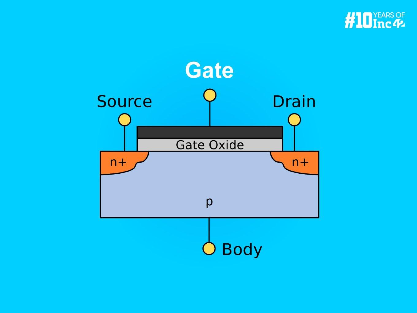
What Is A Semiconductor Gate?
The gate electrode is a thin film of a conductive material deposited on top of an insulator layer in a transistor. The gate sits above a channel formed in the main body of the transistor. We can control the current flow through the transistor by applying a voltage to the gate. This ability to turn current on and off allows transistors to function as electronic switches.
The gate has historically been made of Polysilicon, but metals like Tantalum (Ta) and Tungsten (W), or a Nitride layer (TaN) are becoming more common for modern transistors.
How Does A Gate Function?
As mentioned above, a gate electrode in a transistor functions like a controller for current flow. The following is a deeper dive into how it achieves this:
The Electric Field Effect:
- Insulated Gate: The key to the gate’s control lies in the insulating layer, typically silicon dioxide (SiO2), separating it from the channel. This insulation prevents direct current flow between the gate and the channel.
- Electric Field Creation: When a voltage is applied to the gate electrode, it creates an electric field across the thin insulating layer. This electric field doesn’t directly push current through the channel but influences the channel’s ability to conduct electricity.
- Charge Carrier Manipulation (NMOS example): In an N-type metal-oxide-semiconductor transistor (NMOS), the channel is filled with the majority of charge carriers: electrons.
When a positive voltage is applied to the gate, it attracts electrons towards the channel from a nearby reservoir. This creates a region rich in electrons near the gate, called an inversion layer. The stronger the positive voltage, the more electrons are attracted, forming a thicker inversion layer and allowing current to flow more easily through the channel (transistor turns “on”).
- Opposite Effect In PMOS: In a P-type metal-oxide-semiconductor transistor (PMOS), the channel is filled with the majority of charge carriers called holes.
Applying a positive voltage to the gate in a PMOS transistor repels these holes away from the channel, effectively reducing the number of available charge carriers. This creates a depletion region and hinders current flow (transistor turns ‘off’).
- Gate Voltage as a Switch: By adjusting the voltage applied to the gate, we essentially control the formation of the conductive layer (inversion layer in NMOS) or depletion region. With a sufficient positive voltage (NMOS) or appropriate voltage depending on the transistor type, the gate allows current to flow freely (transistor ‘on’). Conversely, with a specific voltage (usually zero or a negative voltage depending on the transistor type), the gate restricts current flow (transistor ‘off’).
This switching ability forms the base for building digital circuits where transistors act as electronic switches.
What Are The Applications Of Gates In Semiconductors?
The ability to turn current ‘on’ and ‘off’ is the foundation for various gate functionalities in transistors:
- Amplification: Transistors can amplify weak electrical signals. A larger change in the current flowing through the channel can be created by applying a small voltage change to the gate. This is crucial for building amplifiers in many electronic devices.
- Switching: The gate acts as a switch, controlling current flow. This switching ability is the basis for digital circuits. Logic gates, built by combining transistors in specific ways, perform basic logical operations (AND, OR, NOT) using these on/off states. These logic gates are the fundamental building blocks of CPUs, memory chips, and other digital components.
- Signal Processing: Transistors with gates can be used to process analogue signals. The amplitude, frequency, or other characteristics of an analogue signal can be controlled by adjusting the gate voltage.


