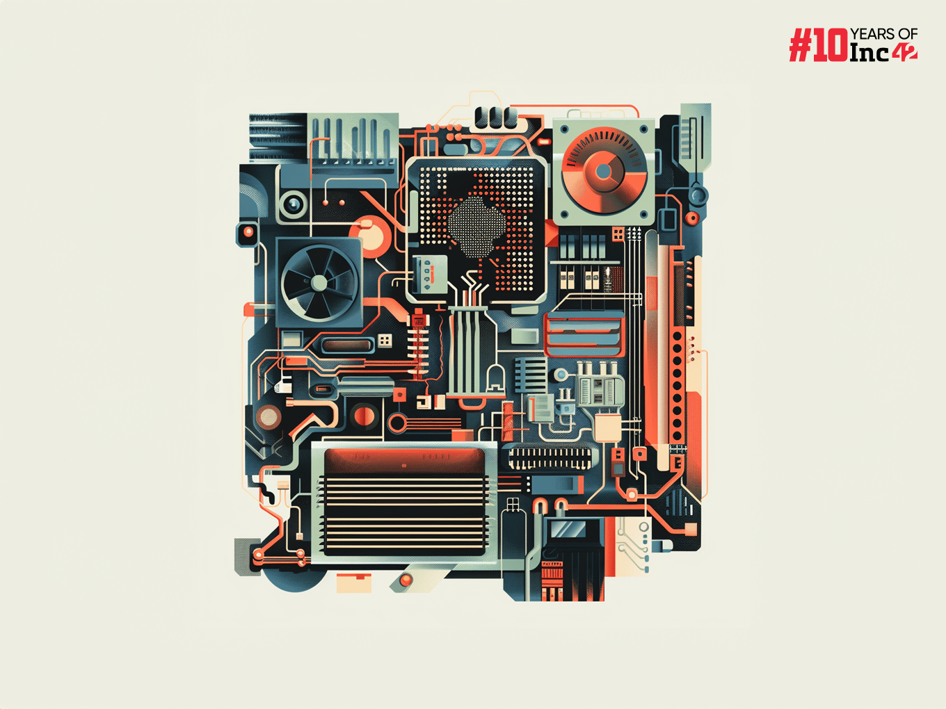
What Is A Printed Circuit Board (PCB)?
A printed circuit board (PCB), also called a printed wiring board (PWB), is a thin board made of insulating material that has thin layers of metal (usually copper) bonded to it.
These metal layers have etched patterns creating electrical pathways connecting electronic components soldered onto the board. The insulating material keeps the electrical traces from touching each other and causing short circuits.
Ideated by Paul Eisler in 1936, PCBs are essential in all modern electronic devices and have caused a paradigm shift in electronics ever since mass usage began post-World War II.
How Is A Printed Circuit Board (PCB) Manufactured?
While manufacturing a PCB involves several precise steps, the following is a simplified breakdown of the process:
- Design & Preparation: The process starts with designing the PCB layout using specialised software. This layout defines the placement of electrical components and the pathways that connect them. A special photoresist film is then applied onto the copper-clad laminate base material.
- Imaging: A plotter, a high-precision printer, creates a film negative of the circuit design on the photoresist film. Areas representing copper traces remain covered, while the rest is exposed.
- Etching: The PCB panel is dipped into an etching solution. This solution erodes the exposed copper, leaving behind the desired circuit pattern on the board.
- Drilling & Plating (Multilayer PCBs only): For PCBs with multiple conductive layers, tiny holes are drilled through the board to allow electrical connections between layers. These holes are then plated with copper to create conductive pathways.
- Lamination (Multilayer PCBs only): Multilayer PCBs involve stacking and bonding separate pre-etched layers using heat and pressure.
- Testing & Finishing: The completed PCB undergoes electrical testing to ensure proper functionality and identify defects. Finally, a protective solder mask and silkscreen markings are applied to the board. The former prevents the solder from sticking to unwanted areas, while the latter labels the components.
Why Are Printed Circuit Boards (PCBs) Important In Electronics?
Printed circuit boards (PCBs) are fundamental to modern electronics for several reasons:
- Connectivity: They provide a reliable and organised way to interconnect electronic components. The etched copper traces act like miniaturised wires but on a flat surface. This allows for precise connections between components and eliminates the messy tangle of cables you’d see in older electronics.
- Miniaturisation: PCBs enable significant size reduction in electronic devices. Compared to bulky point-to-point wiring, PCBs can pack a much higher density of connections into a smaller space. This is crucial for making our devices portable and sleek.
- Standardisation & Mass Production: PCBs allow for standardised designs and efficient mass production. Once the PCB layout is finalised, numerous boards can be fabricated simultaneously, reducing costs and ensuring consistency.
- Reliability: PCBs offer a more robust and reliable method of connecting components than traditional wiring. They are less prone to connection issues or malfunctions with loose wires.
- Versatility: PCBs can be designed in various configurations with single, double, or even multiple copper layers. This allows for building complex circuits with several functions on a single board.
- Protection: The PCB provides physical protection for the mounted delicate electronic components.


