What Is Immersion Lithography?
In semiconductor manufacturing, immersion lithography creates smaller and more intricate features on wafers. It enhances the resolution and precision of the lithography process. Immersion lithography has been instrumental in pushing the boundaries of chip miniaturisation. It has enabled the creation of features below 45 nanometres (nm), which is crucial for modern high-performance processors.
How Does Immersion Lithography Work?
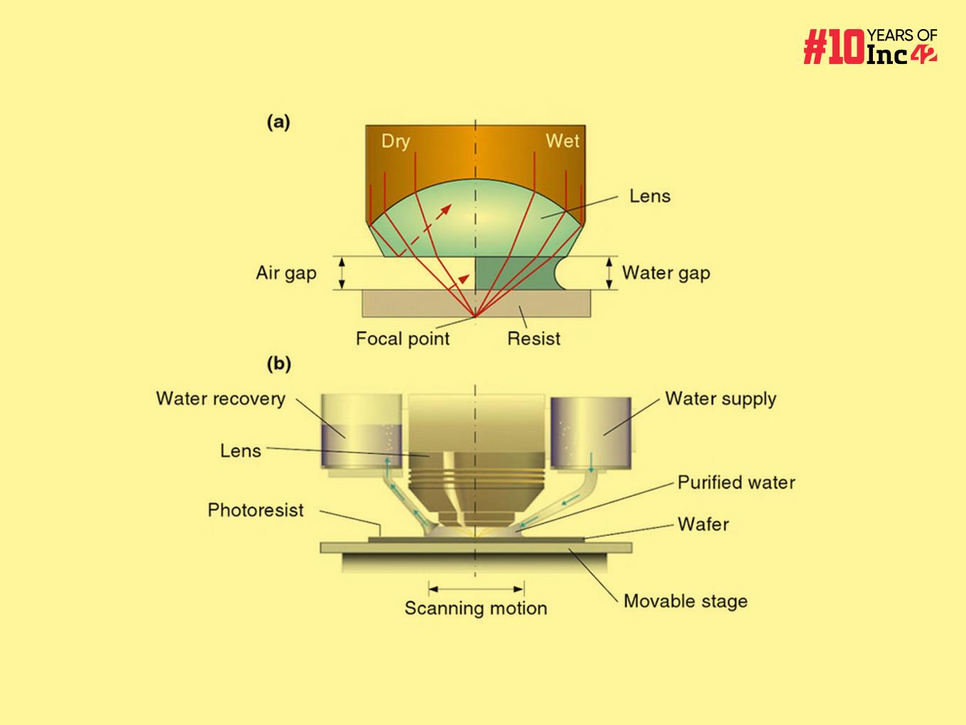
Immersion lithography achieves higher resolution by bending the rules of light a bit. Here’s a breakdown of the key aspects:
- Light & Resolution: In lithography, light transfers a pattern from a photomask onto a photoresist on the wafer. The minimum size of features that can be created depends on the wavelength of light used and the property of the lens system called the numerical aperture (NA).
- Numerical Aperture (NA): NA determines how much light is captured and focussed onto the wafer. It is a measure of the light cone’s angle entering the photoresist. A higher NA allows for the creation of smaller features.
- Air Gap Limitation: Traditionally, air fills the gap between the final lens and the wafer. But, air has a refractive index of 1, which limits how much light can be bent by the lens system, restricting the achievable NA.
- Water To The Rescue: Immersion lithography replaces the air gap with a liquid, usually ultrapure water. Water has a refractive index of around 1.44. This higher index allows the lens to bend light more effectively, increasing the NA.
- Sharper Image: With a higher NA, light can be focussed into a tighter pattern on the photoresist. This translates to creating smaller features on the wafer with greater precision.
What Are The Advantages & Disadvantages Of Immersion Lithography?
While immersion lithography holds promise, it comes with a set of pros and cons worthy of consideration:
Advantages Of Immersion Lithography
- Higher Resolution: The core advantage of immersion lithography is its ability to achieve significantly higher resolution than traditional dry lithography (using air). This is due to the increased numerical aperture (NA) achieved by using a high refractive index liquid like water. With higher resolution, manufacturers can create smaller and more intricate features on chips, which translates to faster and more powerful processors.
- Improved Depth Of Focus (DOF): Immersion lithography offers a deeper depth of focus (DOF) than dry lithography. DOF refers to the acceptable range of distance between the lens and the wafer where a sharp image is projected. This improved DOF allows for more even patterning across the entire wafer surface, reducing manufacturing defects.
- Reduced Reliance On Resolution Enhancement Techniques (RET): Due to the inherent resolution boost, immersion lithography can lessen the need for complex RET methods. RET techniques are computational processes used to correct light diffraction effects that limit resolution in traditional lithography. Simplifying the process can lead to faster turnaround times and lower costs.
- Improved Critical Dimension Uniformity (CDU): CDU refers to the variation in the size of features across a wafer. Immersion lithography helps achieve better CDU compared to dry lithography. This uniformity is crucial for consistent chip performance.
Disadvantages Of Immersion Lithography
- Complexity & Cost: The immersion system adds complexity to the lithography tool compared to dry lithography. Maintaining a clean and debris-free environment for the high-purity water used in the immersion process also adds to the cost.
- Environmental Concerns: Water disposal after use requires careful treatment to avoid contamination.
- Limited Scalability: As feature sizes continue to shrink, the effectiveness of immersion lithography eventually reaches a limit. Researchers are exploring alternative immersion liquids with even higher refractive indices or next-generation techniques like EUV (extreme ultraviolet) lithography.


