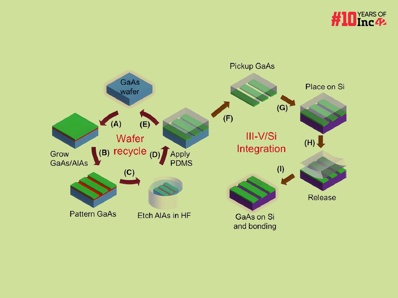
What Is Epitaxial Growth?
Epitaxial growth is a fundamental process in semiconductor manufacturing. It refers to depositing a thin, crystal layer on a crystal substrate, with a specific orientation. This layer closely resembles the crystal structure of the underlying substrate, like stacking identical building blocks.
What Are The Two Types Of Epitaxial Growth?
There are two main types of epitaxial growth distinguished by the material composition of the deposited layer relative to the substrate:
- Homoepitaxy: In this type, the deposited layer has the same chemical composition as the substrate. It’s like adding another layer of the same material onto an existing foundation. This technique is often used to achieve a purer layer on top of a substrate or obtain a specific thickness for a particular device layer.
- Heteroepitaxy: The deposited layer has a different chemical composition than the substrate. This allows for creating structures with unique material combinations. However, achieving a perfect crystalline alignment between the layer and substrate can be more challenging due to the material difference.
How Is Epitaxial Growth Achieved?
Epitaxial growth can be achieved through several techniques, all of which involve supplying a source of material and precisely controlling the conditions for it to deposit onto a substrate in a crystal structure that aligns with the underlying crystal. Here are three main methods:
- Molecular Beam Epitaxy (MBE): This method utilises an ultra-high vacuum environment. Source materials are heated to create beams of atoms or molecules travelling towards a precisely positioned substrate. The atoms or molecules arrange themselves on the substrate’s surface, replicating its crystal structure layer by layer. MBE offers excellent control over the deposition process and is ideal for creating complex structures with precise thicknesses and doping profiles.
- Chemical Vapour Deposition (CVD): In CVD, the source material is introduced as a gas or a vapour. This gas reacts with the hot substrate’s surface, breaking down and leaving behind the desired atoms that build the epitaxial layer. CVD offers a wider range of materials that can be deposited compared to MBE and is generally a faster process. However, it may have less precise control over the layer’s composition and thickness.
- Liquid Phase Epitaxy (LPE): This method uses a molten source material, often a metal or a compound semiconductor solution, that comes in contact with the substrate. The growth occurs at the interface between the liquid and the solid substrate. LPE is particularly useful for growing thick layers and can be less expensive than other techniques. However, controlling the uniformity of the deposited layer may be more challenging.
Why Is Epitaxial Growth Used In Semiconductor Manufacturing?
Epitaxial growth is a critical process in semiconductor manufacturing for several reasons:
- High-Purity Layers: The epitaxial layer can be grown with higher purity than the bulk substrate material. This is because the deposition process allows for better control over impurities and defects. This improved purity translates to better electrical performance and device characteristics.
- Precise Doping Profiles: Doping refers to intentionally introducing impurities into a semiconductor to control its electrical conductivity. Epitaxial growth allows for creating layers with very specific doping profiles, essential for crafting the desired functionality of transistors and other semiconductor devices.
- Tailored Material Properties: Engineers can achieve specific electrical or optical properties by using different materials for the epitaxial layer compared to the substrate (heteroepitaxy). This enables the creation of advanced devices like lasers, light-emitting diodes (LEDs), and high-performance transistors.
- Strained Silicon Layers: Epitaxy allows for creating layers with a slightly distorted crystal lattice structure compared to the substrate (strained silicon). This strain can improve the mobility of charge carriers within the device, leading to faster and more efficient transistors.
- Defect-Free Interfaces: Epitaxial growth ensures a smooth and defect-free interface between the layer and the substrate. This is crucial for efficient electron and hole movement within the device and overall device performance.


