What Is Doping?
Doping in semiconductors is adding a small amount of impurities into a very pure semiconductor material. It might sound strange to add impurities on purpose, but this is a critical to make semiconductors useful in electronics.
What Are The Types Of Doping?
There are two main types of doping in semiconductors:
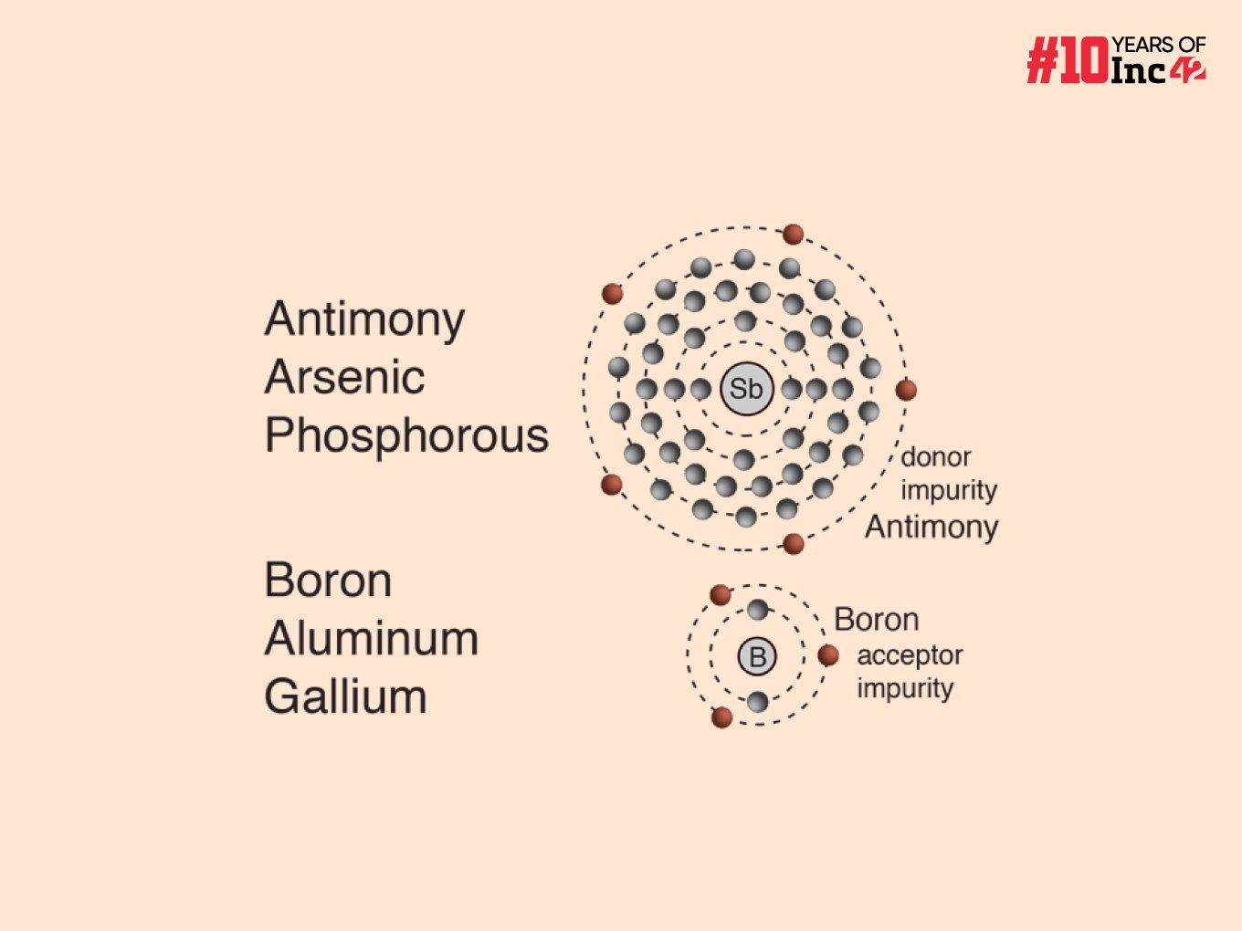
N-type doping: This involves adding elements with five valence electrons to a semiconductor, such as silicon or germanium. These elements are typically from Group V of the periodic table, common examples being phosphorus (P), arsenic (As) and antimony (Sb).
When one of these elements is added to the semiconductor lattice, four of their valence electrons form bonds with the surrounding silicon atoms. However, the fifth valence electron remains loosely bound and can be easily excited into the conduction band. This creates an excess of negative charge carriers (electrons) in the material, making it more conductive.
P-type doping: This process introduces elements with only three valence electrons into the semiconductor. These dopant elements come from Group III of the periodic table, with boron (B) being the most common choice for silicon.
Here, the dopant atom creates bonds with neighbouring silicon atoms but lacks one electron to complete the bonding. This creates a ‘hole’ where an electron allows neighbouring electrons to move around and fill this hole. This movement of holes acts like a positive charge carrier flow, giving the material p-type conductivity.
How Is Doping Achieved?
Doping can be achieved through several methods, but two of the most common are diffusion and ion implantation. The following is a brief description of how they work:
Diffusion
- In this method, the dopant material, often in a gas or a solid source, is introduced into a high-temperature environment within the semiconductor wafer.
- At these high temperatures (typically 1000-1250°C), the dopant atoms diffuse from the high concentration area (source) into the semiconductor crystal lattice, which has a lower concentration of dopant atoms.
- This process typically involves two stages:
- Pre-deposition: The dopant material is deposited onto the wafer surface.
- Drive-in: The wafer is heated again, allowing the dopant atoms to diffuse deeper into the semiconductor.
Ion Implantation
This method uses an accelerated beam of ionised dopant atoms (ions) to implant them directly into the semiconductor crystal lattice. The ions are precisely controlled in energy and direction, allowing for a more controlled doping profile than diffusion.
Ion implantation offers advantages like better control over dopant concentration and depth. However, it is a more complex and expensive process than diffusion.
How Does Doping Help Semiconductors?
Doping is the key that unlocks the potential of semiconductors, transforming them from mediocre conductors into the foundation of modern electronics. The following are the reasons why doping is a fundamental step in manufacturing semiconductor-based electronics:
- Controllable Conductivity: Pure (intrinsic) semiconductors are neither great conductors nor insulators. They occupy an awkward middle ground. Doping allows for precise control over the material’s conductivity. By introducing specific impurities (dopants), we can either create n-type or p-type semiconductors:
- N-type semiconductors with extra mobile electrons become better conductors.
- P-type semiconductors with an abundance of “holes” (places where electrons could be) also conduct electricity but in a different way.
- Building Blocks For Electronic Devices: The magic happens when n-type and p-type semiconductors are combined in specific configurations. These junctions between differently doped regions form the foundation of essential electronic components like:
- Transistors: The workhorse of modern electronics, transistors act as switches or amplifiers by controlling the current flow through these doped regions.
- Diodes: These components allow current to flow in one direction more easily than the other, crucial for various functions in circuits.
- Tailoring Properties: Doping allows for tailoring electrical properties of semiconductors for specific applications. Here are some examples:
- Higher Conductivity: For applications requiring higher current flow, like power electronics, heavily doped semiconductors can be used to minimise resistance.
- Light-Emitting Diodes (LEDs): Doping with specific elements allows for control over the energy levels of electrons and holes, influencing the wavelengths of light emitted by LEDs.


