What Is Chemical Mechanical Polishing?
Chemical mechanical polishing (CMP) or chemical mechanical planarization (CMP), is a technique used to smoothen and flatten surfaces at the nanoscale level. It is particularly important in manufacturing integrated circuits, where microscopic features have to be precisely formed on a perfectly flat surface.
CMP offers several advantages over other techniques:
- Planarization: It can achieve a very high degree of flatness, which is crucial for subsequent processing steps in chip manufacturing.
- Selective Removal: The chemical component allows for the targeted removal of specific materials, leaving desired features behind.
- Minimal Damage: Compared to purely mechanical polishing, CMP minimises surface defects.
How Is Chemical Mechanical Polishing Done?
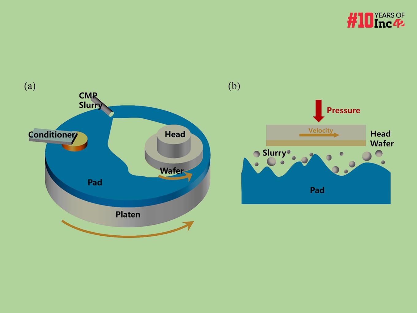
Chemical mechanical polishing (CMP) involves a delicate interplay between mechanics and chemistry to achieve a super-flat surface. Here’s a breakdown of the process:
- Preparation: The wafer or substrate is secured onto a holder designed for CMP.
- Slurry Application: A special chemical slurry is dispensed onto a rotating polishing pad. This slurry is the heart of CMP, containing:
- Abrasive Particles: These microscopic particles physically grind down the surface irregularities. Their size and type are chosen based on the material being polished.
- Reactive Chemicals: These chemicals soften the polished material, allowing the abrasives to work more efficiently. They can also be formulated for selective removal of specific materials.
- Polishing: The wafer holder presses the wafer down onto the spinning polishing pad. The combination of:
- Mechanical force: Applied by the pressing head
- Friction from the pad’s rotation
- Chemical action of the slurry
- Shearing forces as the wafer slides across the pad removes material from the wafer’s surface.
- In-situ monitoring: Throughout the process, various sensors monitor factors like material removal rate, uniformity, and surface quality. This allows for adjustments to be made in real time for optimal results.
- Cleaning & Inspection: After polishing, the wafer is thoroughly cleaned to remove residual slurry or contaminants. Finally, the wafer’s surface is inspected for uniformity, flatness, and defects introduced during CMP.
Why Is Chemical Mechanical Polishing Used In Manufacturing Integrated Circuits?
There are several key reasons why chemical mechanical polishing (CMP) is crucial in manufacturing integrated circuits (ICs):
- Planarization For Multi-Layered Circuits: Modern ICs are not simply flat circuits with components etched on a single surface. They are intricate structures with multiple layers of transistors, conductors, and insulators deposited atop each other.
CMP ensures that each layer is deposited on a perfectly flat surface. This is critical because subsequent lithography steps, which define circuit patterns using light, rely on a uniform surface for precise patterning. Even minor bumps or dips can distort the patterns and lead to malfunctioning circuits.
- Enabling Multi-Level Interconnects: Transistors and other components in an IC need to be electrically connected. CMP helps create these connections by precisely polishing away specific materials between layers, exposing lower layers and allowing for the formation of vias (holes) and trenches for metal interconnects. This enables the complex 3D architecture of modern ICs.
- Surface Quality For Patterning: A smooth and defect-free surface is essential for subsequent patterning steps using photolithography. CMP minimises surface roughness and reduces defects that could interfere with the precise etching of circuit features.
- Selective Material Removal: The ability of CMP to selectively remove certain materials allows for precise control over the final topography of the wafer. This is crucial for creating features like shallow trench isolation (STI), which separates transistors on the chip.


